PCB Gerber File Checklist
Requirements for files:
- Gerber files (RS-274D or RS-274X preferred) including
- Excellon Drill File
- Drill Tool List (sometimes embedded in Drill File)
- Top and Bottom Copper Layers (positive polarity)
- Inner layers (polarity based on design) (4 layer only)
- Top and Bottom Soldermask (negative polarity – presence of data will represent the absence of soldermask on the board. Outline only will cover the board entirely with soldermask)
- Top and /or Bottom Silkscreen (positive polarity) silkscreen files are optional
- Board Outline (if not already present on another layer)
- Aperture / D-Code List (if file set is not RS-274X compliant)
- All PCB holes are viewed from the top layer of the board
- All holes will be treated as through holes. (no blind or buried vias)
- Files are contained in a single compressed file (.zip) containing only the required files. No other compressed file types accepted.
- Once an order is submitted into process no additional changes to the files will be permitted
- *Print notes, readme and other such documentation will be ignored in the process of building your orders.
*Do not assume what you see in your design software is what you get in the exported Gerber. It is wise to perform a final proof reading of your Gerber output before sending them. To do this you will need a Gerber viewer to view your files graphically. Some design software have this capability built in. If this is not an option, we recommend looking at Gerbv. It is a free open source option; it does not have any commercial use restrictions, and is easy to use. Pay special attention to ground fills, intended connections to the ground fills and outlines.
Layer Naming Recommendations:
When providing your Gerber files please make sure to use the recommended naming conventions shown below for your layers. If the layer stack-up for your order is unidentifiable your order may be cancelled. Here are some naming conventions based on popular CAD tools that would help us to identify how to build your PCB:
| Layer Naming Guide – 2 Layer | ||||||
| Drill | txt | drl | drd | dri | xln | ncd |
| Top Copper | gtl | cmp | top | L01 | art1 | |
| Bottom Copper | gbl | sol | bot | L02 | art2 | |
| Top Soldermask | gts | stc | smt | psm | gtm | |
| Bottom Soldermask | gbs | sts | smb | ssm | gbm | |
| Top Silk | gto | plc | slk | pss | sst | |
| Bottom Silk | gbo | pls | bsk | sss | ssb | |
| Outline | oln | otl | gm1 | gko | ddw | |
| Layer Naming Guide – 4 Layer | ||||||
| Drill | txt | drl | drd | dri | xln | ncd |
| Top Copper | gtl | cmp | top | L01 | art1 | |
| Inner Layer 1 | in1 | mid1 | ||||
| Inner layer 2 | in2 | mid2 | ||||
| Bottom Copper | gbl | sol | bot | L04 | art4 | |
| Top Soldermask | gts | stc | smt | psm | gtm | |
| Bottom Soldermask | gbs | sts | smb | ssm | gbm | |
| Top Silkscreen | gto | plc | slk | pss | sst | |
| Bottom Silkscreen | gbo | pls | bsk | sss | ssb | |
[*In the event that you use an alternate naming convention we will create a layer stack for you.]
Requirements for Drill File:
- Must be submitted in Excellon format
- Must be ASCII text viewable. Please open with “Word” or “notepad” to verify a numeric list of X & Y coordinates. (There should be no strange graphical characters)
- PCB drill files should not contain “G01”, “G54” and/ or reference to “D” codes when opened in a text editor. (This indicates a Gerber format and is most likely a drill drawing rather than an NC file output)
- Properly formatted PCB Drill files have sizes separated with “T” codes that indicate tool numbers. (T01, T02, etc.) tool report with the drill sizes necessary (if not contained in the drill file header).
- The largest drill size available is a 0.257″.
- Drill/Fab Drawings cannot be used in place of Excellon drill files.
*Below we have included an example of a properly formatted NC Drill file. A properly formatted NC Drill file will have X & Y Coordinates with tool sizes viewable in any text editor. It is this file that governs your finished holes sizes and locations.
Example of properly formatted NC Drill File:
M48
T01C0.020
T02C0.028
T03C0.030
T04C0.032
T05C0.035
T06C0.040
%
T01
X01944Y00642
X01991Y00877
X01907Y00923
X01537Y01095
X01622Y01357
X01752Y01391
X01668Y01504
X01498Y01498
PCB Routing Restrictions:
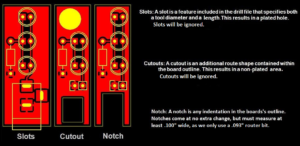
- Notches in board edge must be 0.100” or larger with a minimum 0.050” radius at the end.
- EasyPCB uses only a 0.093” router bit to keep costs low.
- Any notch smaller than 0.100” may result in nearby features being routed into and damaged.
- Any board edge notch that is not a straight in and out (any turns or bends) will result in a canceled order.
- Slots or cutouts contained in the outline layer will be ignored.
- Outlines will be processed “as is” and even the slightest imperfection in the Gerber data can cause some issues with arcs and notches.
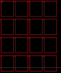
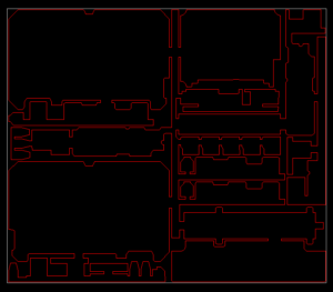
- Customers must submit their PCB designs as a single board. For designs submitted where there are multiple boards or designs with a complex route path aimed at tabbing these boards into an array, EasyPCB has the discretion to cancel these orders and refund the charges. (Examples shown below)


Perimeter PCB Routing Details:
Our automated process will program the circuit board routing by reading the path of your outline. The outline must be a continuous line. The board dimensions are determined from the center of the line used to draw the outline and will be routed to a +/- 0.010″ tolerance. You should leave 0.020″ space from the routed edge of the board to the nearest copper feature to avoid any inadvertent damage that could be a result of the routing tolerance..
Items that can cause an order Cancellation:
Missing Layer:
- Copper layers
- If the number of layers is not what is provided on the order form (2 or 4)
- If your design contains circuitry on only one side (“single sided”) you must still provide two copper layers (one as pads only for the drilled holes). All orders will go through the standard plating process-holes will have plating in the barrels.
- Missing layers will result in a cancellation.
- Drill file
- If your order is missing a drill file, your order will be cancelled. *Unless the order clearly has no need for a drill file.
- Outline
- If you are missing an outline we will create a rectangular outline to match your ordered board size, centered about the data.
- If there are copper features outside of the created outline as mentioned above, the order will be cancelled.
- Soldermask
- Two soldermask layers are required, otherwise the order will be cancelled.
- If circuitry is only present on one side (“single sided”) you must still provide two soldermask layers (this can be an “outline only” to flood bare side with soldermask, or a “solid block” which will remove the soldermask from that side) Missing layers will result in a cancellation.
- Silkscreen (none, one, or two)
- Since EasyPCB pricing includes up to two silkscreen layers, we will run with whatever is present in the file set.
- Very small features will wash away-we will not be “bumping” the size-please view in a Gerber editor.
- We will be performing an automated “clip” using the soldermask layer to remove silkscreen from solderable surfaces.
- Please draw silkscreen traces, elements, and logos with lines measuring at least 0.003”. Anything measuring smaller may not be visible after manufacturing. Logos in silkscreen can be particularly problematic at times. Inspect these in your Gerber viewer looking for fills made with very small line segments >0.003″. These often will not print on the PCB and we know that usually your logo is pretty important.
Board Dimension
- A board dimension found in a file that is more than +/- 0.25” from the order form dimension will be cancelled.
- A board dimension > 8.00” in either dimension (length or width) will be cancelled
- A board area that differs > 1.0 in² (per board) than the order form will be cancelled (length x width)
- A board dimension < 0.25” in either dimension (length or width) will be cancelled
- A board area greater than 30.0 in² will be cancelled. (length x width)
Slots
- Slots created in the drill file with overlapping drills will be cancelled if the hole size is ≤ to 0.070”
- Slots created in the drill file with overlapping drills will not be cancelled if the hole size is > 0.070” but the result of this practice cannot be guaranteed and may not meet your needs.
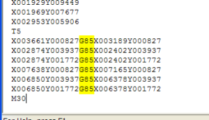
- Slots contained in the drill layer using a G85 command code will be cancelled (Example shown below as viewed in Notepad)

Route Path
- Notches in board edge must be 0.100” or larger with a minimum 0.050” radius at the end.
- EasyPCB uses only a 0.093” router bit to keep costs low.
- Any notch smaller than 0.100” may result in nearby features being routed into.
- Any board edge notch or key slot that is not a straight in and out (any turns or bends) will be cancelled.
- Slots or cutouts contained in the outline layer will be ignored.
